Home >> Satellite 1 (Department of Metallurgy, Materials Science and Materials Processing)
Instruments of Satellite 1
| XPS | EPMA | AES |
| GD-OES | XRF |
| TEM1, TEM2, TEM3 | FE-SEM1, FE-SEM2, FE-SEM3, FE-SEM4 | Focused Ion Beam Scanning Electron Microscope | |
| Ion milling | FIB sample finishing equipment | AES |
| NMR (600MHz, 400MHz,300MHz) |
SEARMS room
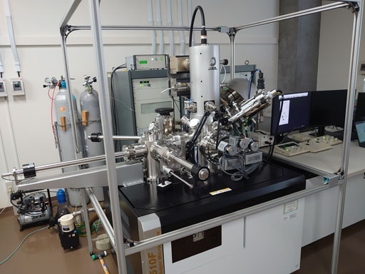
XPS (X-ray Photoelectron Spectrometer)
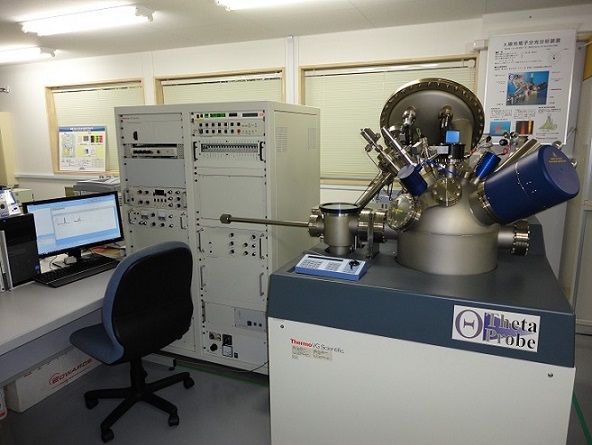
| Model | ThermoFisher Scientific, Theta Probe |
|---|---|
| X-ray Source | Monochromated, Al Kα |
| X-ray spot size | ⌀200µm (min. ⌀15µm) |
| Spectrometer | Hemispherical analyzer (SCA) |
| Angle resolution measurement | Maximum 96 divisions (sample inclination is unnecessary) |
| Detection depth | A few nm or less (surface area) |
| Size of sample | 70mm × 70mm × 25mm (max.) |
| Target element | Li - |
| Accesary devices | Angle resolving measurement, neutralizing gun |
| Applications | Detect and separate the photoelectrons generated when the sample is irradiated with X-rays, and qualitatively analyze each element on the material surface and measure the chemical composition on the surface. |
| Person in charge | Akao, Ohira |
| Notes | Please contact the person in charge in advance to consult with us. This equipment is managed and operated by the Instrumental Analysis Group on commission from the "Department of Metallurgy, Materials Science and Materials Processing". Those who do not belong to "Department of Metallurgy, Materials Science and Materials Processing" staff are required to submit an application form distributed at the first visit. |
EPMA (Electron Probe Microanalyzer)
| Model | JEOL, JXA-8530F |
|---|---|
| Electron gun | Schottky-type field emission (FE) electron gun |
| Number of spectrometer | 5 (crystal spectrometers: 10) |
| Resolution | µm |
| Sample holder | ⌀25mm × 19mmh |
| Element | B - |
| Accesary devices | EDS (B -) |
| Applications | Characteristic X-rays of each element generated when the sample is irradiated with an electron beam are detected, and element mapping and material composition are quantitatively analyzed. |
| Person in charge | Akao, Ohira |
| Notes | Please contact the person in charge in advance to consult with us. This equipment is managed and operated by the Instrumental Analysis Group on commission from the "Department of Metallurgy, Materials Science and Materials Processing". Those who do not belong to "Department of Metallurgy, Materials Science and Materials Processing" staff are required to submit an application form distributed at the first visit. |
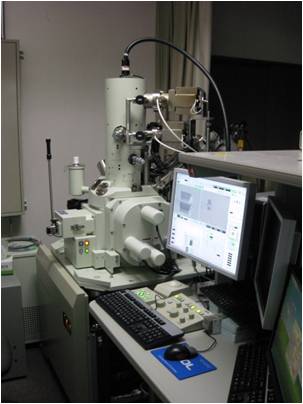
AES (Auger Electron Spectrometer)
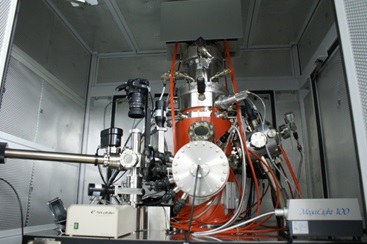
| Model | ULVAC-PHI, PHI 710 |
|---|---|
| Electron gun | Field emission type electron gun |
| Spectrometer | Cylindrical mirror analyzer (CMA) |
| Detection depth | A few nm or less |
| Sample size | 35mm × 35mm × 12mmh (With 2 inch holder) |
| Target elements | Li - |
| Accessory devices | Low Temperature Rupture Transfer vessel High resolution AES spectrum measurement function |
| Applications | Auger electrons generated when a specimen is irradiated with an electron beam are detected, and element mapping is measured. In addition, analysis of the distribution and composition of elements in the depth direction of the material in the sample is performed together with sputter etching. |
| Person in charge | Ohira, Akao |
| Notes | Please contact the person in charge in advance to consult with us. This equipment is managed and operated by the Instrumental Analysis Group on commission from the "Department of Metallurgy, Materials Science and Materials Processing". Those who do not belong to "Department of Metallurgy, Materials Science and Materials Processing" staff are required to submit an application form distributed at the first visit. |
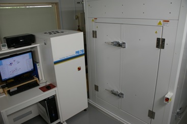
GD-OES (Glow discharge optical emission spectrometer)
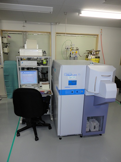
| Model | HORIBA JOBIN YVON, GD-Profiler 2 |
|---|---|
| Lamp | Marcus type |
| Anode diameter | ⌀4mm (standard) |
| Spectrometer | Polychrometer (45), monochromator (1) |
| Depth resolution | nm order |
| Sample size | More than ⌀10mm |
| Target elements | H - |
| Accessory devices | Small sample measuring device |
| Applications | The sample is sputter-etched by high-frequency pulsed glow discharge, and the sputtered particles released from the sample are excited and emitted in the glow discharge, and spectroscopic analysis is performed to qualitatively and quantitatively analyze the elements in the depth direction. |
| Person in charge | Ohira, Akao |
| Notes | Please contact the person in charge in advance to consult with us. This equipment is managed and operated by the Instrumental Analysis Group on commission from the "Department of Metallurgy, Materials Science and Materials Processing". Those who do not belong to "Department of Metallurgy, Materials Science and Materials Processing" staff are required to submit an application form distributed at the first visit. |
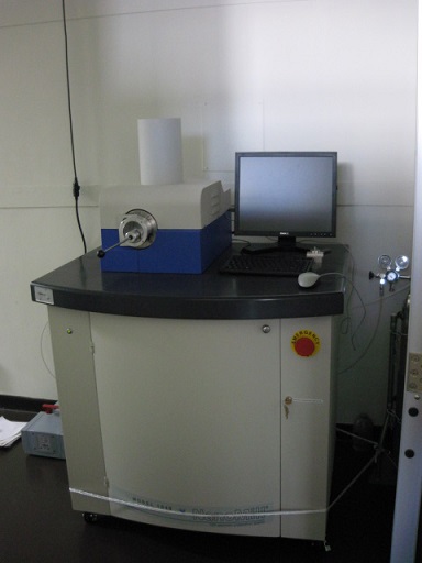
XRF (X-ray Fluorescence analyzer)
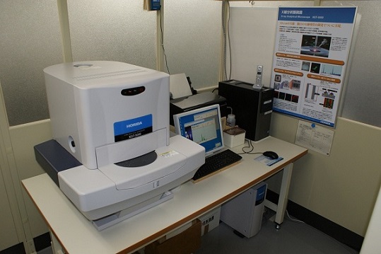
| Model | HORIBA, XGT-5000 |
|---|---|
| X-ray spot size | ⌀10µm, ⌀100µm |
| Maximum measurement area | 100mm × 100mm |
| Energy range | 0 - 40keV |
| Mapping area | 512µm × 512µm - 100mm × 100mm |
| Target elements | Na - |
| Accessory devices | XY scanning stage Transmission X-rays imaging |
| Applications | Scanning while irradiating the material with X-rays narrowed down by X-ray conduit with ⌀10 µm or ⌀100 µm and perform elemental analysis, element mapping and structural analysis of the sample by transmission X-ray imaging or fluorescent X-ray measurement. |
| Person in charge | Ohira, Akao |
| Notes | Please contact the person in charge in advance to consult with us. This equipment is managed and operated by the Instrumental Analysis Group on commission from the "Department of Metallurgy, Materials Science and Materials Processing". Those who do not belong to "Department of Metallurgy, Materials Science and Materials Processing" staff are required to submit an application form distributed at the first visit. |
Electron microscope room
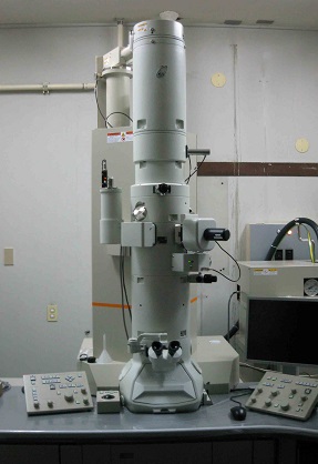
TEM (Transmission Electron Microscope)
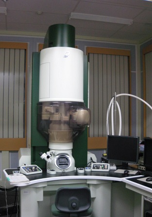
| Model | JEOL, JEM-ARM200F |
|---|---|
| Accelerating voltage | 200, 120kV |
| Resolution (particle image) | 0.08nm (STEM), 0.19nm (TEM) |
| Electron gun | Hot cathode field emission gun |
| Sample inclination angle | ±25° |
| Accessory devices | Energy dispersive X-ray spectrometer (EDX) Electron energy-loss spectroeter (EELS) STEM ADF/BF detector Bottom mounted CCD camera |
| Applications | Morphological observation, structure analysis, composition analysis at micro regions. |
| Person in charge | Kobayashi |
| Notes | Please contact with the person in charge by e-mail when using. This equipment is managed and operated by the Instrumental Analysis Group on commission from the "Department of Metallurgy, Materials Science and Materials Processing". |
TEM (Transmission Electron Microscope)
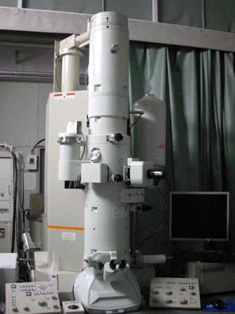
| Model | JEOL, JEM-2100 (HR) |
|---|---|
| Accelerating voltage | 200kV |
| Resolution (particle image) | 0.23nm |
| Electron gun | LaB6 electron gun |
| Acceptance angle | X:±35° Y:±30° |
| Accessory devices | Energy dispersive X-ray spectrometer (EDX) STEM detector Bottom mounted CCD camera |
| Applications | Morphological observation, structure analysis, composition analysis at micro regions. |
| Person in charge | Kobayashi |
| Notes | Please contact with the person in charge by e-mail when using. This equipment is managed and operated by the Instrumental Analysis Group on commission from the "Department of Metallurgy, Materials Science and Materials Processing". |
TEM (Transmission Electron Microscope)
| Model | JEOL, JEM-2100 (HC) |
|---|---|
| Accelerating voltage | 200kV |
| Resolution (particle image) | 0.31nm |
| Electron gun | LaB6 electron gun |
| Acceptance angle | X:±38° Y:±30° |
| Accessory devices | Bottom mounted CCD camera |
| Applications | Morphological observation and structural analysis at micro regions. |
| Person in charge | Kobayashi |
| Notes | Please contact with the person in charge by e-mail when using. This equipment is managed and operated by the Instrumental Analysis Group on commission from the "Department of Metallurgy, Materials Science and Materials Processing". |
FE-SEM (Field Emission Scanning Electron Microscope)
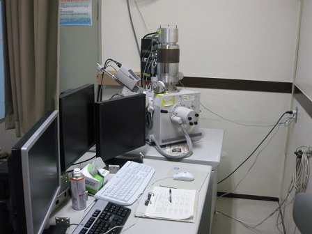
| Model | Philips (FEI) XL-30FEG |
|---|---|
| Accelerating voltage | Max. 30kV |
| Resolution | 2.0nm (30kV) |
| Electron gun | Hot cathode field emission gun |
| Acceptance angle | Max. +75° |
| Accessory devices | Backscattered electron detector Energy dispersive X-ray spectrometer (EDX) Crystal orientation analyzer (TSL) |
| Applications | Morphological observation, structural analysis, composition analysis of sample surface. |
| Person in charge | Kobayashi |
| Notes | Please contact with the person in charge by e-mail when using. This equipment is managed and operated by the Instrumental Analysis Group on commission from the "Department of Metallurgy, Materials Science and Materials Processing". |
FE-SEM (Field Emission Scanning Electron Microscope)
| Model | JEOL, JSM-7800F |
|---|---|
| Accelerating voltage | 0.01 - 30kV |
| Resolution | 0.8nm (15kV), 1.2nm (1kV) |
| Electron gun | Hot cathode field emission gun |
| Acceptance angle | -5 - +70° |
| Accessory devices | Upper detector Backscattered electron detector Crystal orientation analyzer (TSL HIKARI) |
| Applications | Morphological observation, structural analysis of sample surface. |
| Person in charge | Kobayashi |
| Notes | Please contact with the person in charge by e-mail when using. This equipment is managed and operated by the Instrumental Analysis Group on commission from the "Department of Metallurgy, Materials Science and Materials Processing". |
FE-SEM (Field Emission Scanning Electron Microscope)
| Model | JEOL, JXA-8530F |
|---|---|
| Accelerating voltage | 1 - 30kV |
| Resolution | 3.0nm (30kV) |
| Electron gun | Hot cathode field emission gun |
| Accessory devices | Backscattered electron detector Wavelength dispersive X-ray spectrometer (WDX) Energy dispersive X-ray spectrometer (EDX) |
| Applications | Morphological observation, structural analysis of sample surface. |
| Person in charge | Kobayashi |
| Notes | Please contact with the person in charge by e-mail when using. This equipment is managed and operated by the Instrumental Analysis Group on commission from the "Department of Metallurgy, Materials Science and Materials Processing". |
FE-SEM (Field Emission Scanning Electron Microscope)
| Model | JEOL JSM-IT800(SHL) |
|---|---|
| Accelerating voltage | 0.01~30kV |
| Resolution | 0.5nm (15kV),0.7nm (1kV) |
| Electron gun | Hot cathode field emission gun |
| Acceptance angle | -5~+75° |
| Accessory devices | Upper detector Upward hybrid detector Backscattered electron detector Energy dispersive X-ray spectrometer (EDX) Crystal orientation analyzer (TSL Orion) Soft X-Ray Emission Spectrometer(SXES) |
| Applications | Morphological observation, structural analysis, composition analysis of sample surface. |
| Person in charge | Kobayashi |
| Notes | Please contact with the person in charge by e-mail when using. This equipment is managed and operated by the Instrumental Analysis Group on commission from the "Department of Metallurgy, Materials Science and Materials Processing". |
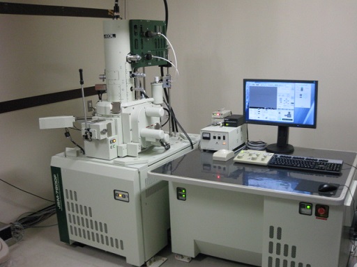
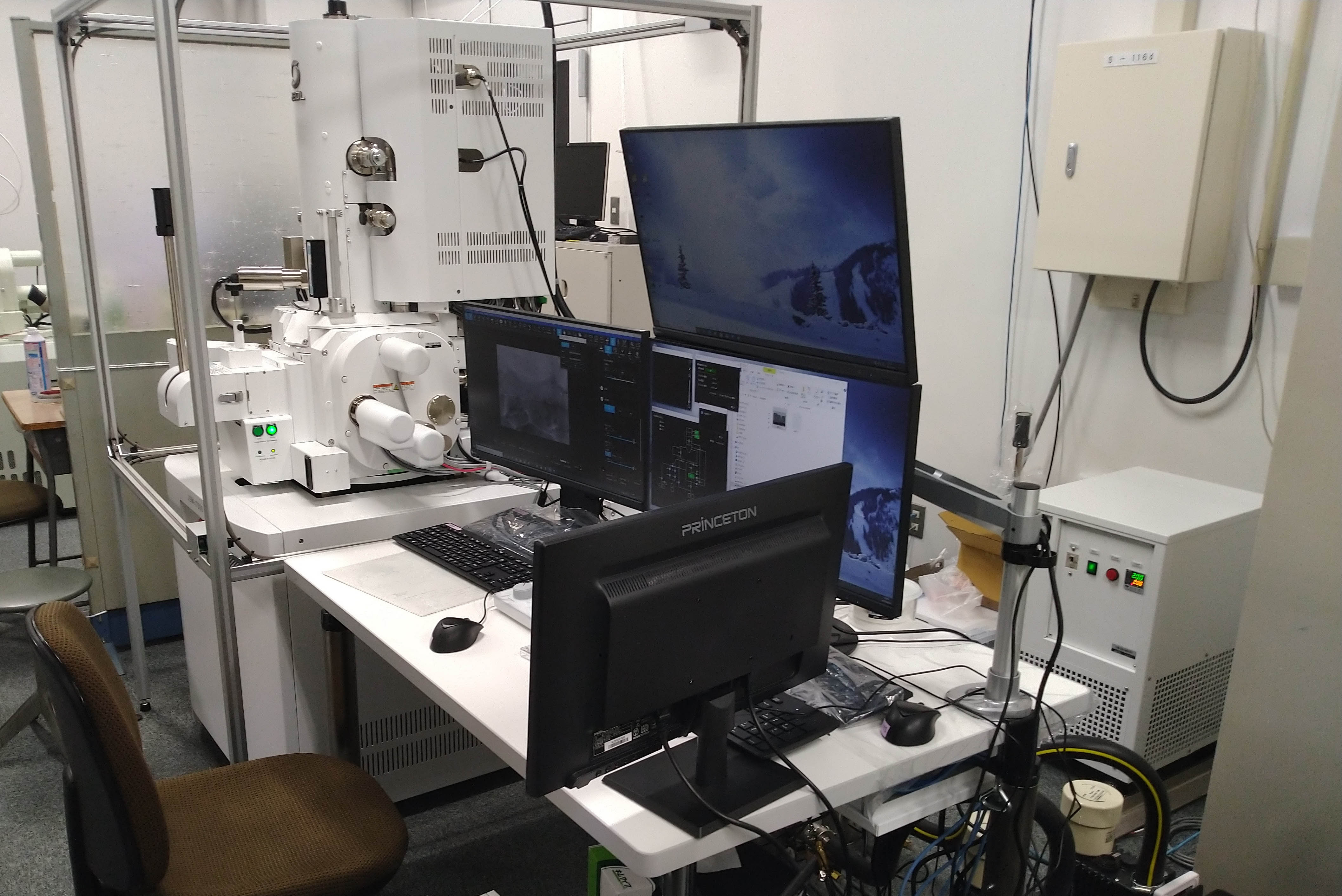
Focused Ion Beam Scanning Electron Microscope
| Model | JEOL, JIB-4600F |
|---|---|
| Accelerating voltage | 0.2 - 30kV (SEM) 1 - 30kV (FIB) |
| Image resolution | 1.2nm (30kV, SEM) 5.0nm (30kV, FIB) |
| Ion source, Electron gun | Hot cathode field emission electron gun (SEM) Ga liquid metal ion source (FIB) |
| Accessory devices | backscattered electron detector EDX Gas injection system (C, W) Nano manipulator system (OmniProbe) Crystal orientation analyzer (TSL) |
| Applications | Morphological observation, structural analysis, composition analysis of sample surface. Sample processing in the micro range. |
| Person in charge | Kobayashi |
| Notes | Please contact with the person in charge by e-mail when using. This equipment is managed and operated by the Instrumental Analysis Group on commission from the "Department of Metallurgy, Materials Science and Materials Processing". |
Ion milling
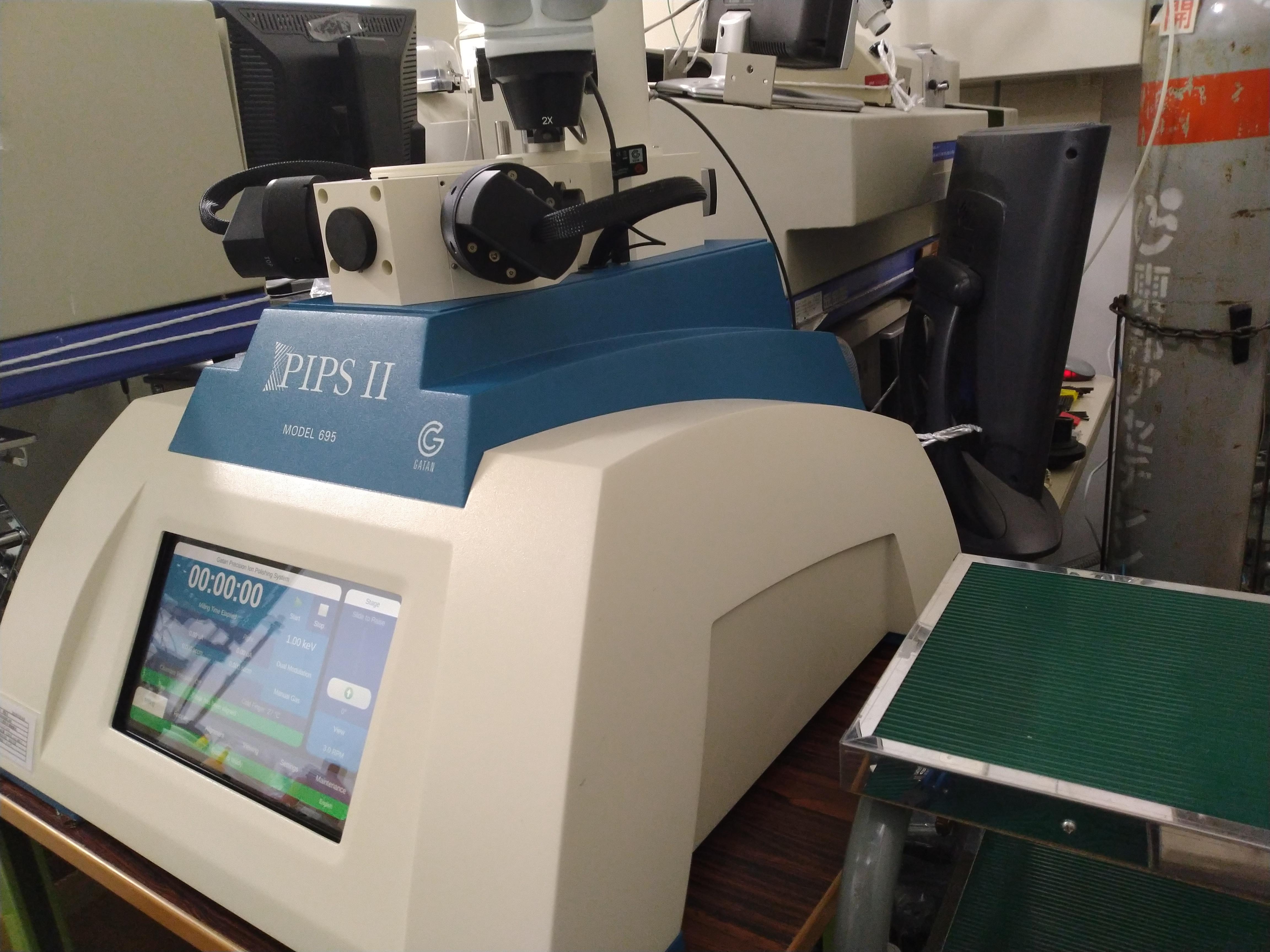
| Model | Gatan PIPSⅡ cool Model695 |
|---|---|
| Gas | Ar |
| Accelerating voltage | Max. 8kV |
| Irradiation angle | ±10° |
| Accessory devices | Cooling processing |
| Applications | Polishing of flaked samples. |
| Person in charge | Kobayashi |
| Notes | Please contact with the person in charge by e-mail when using. This equipment is managed and operated by the Instrumental Analysis Group on commission from the "Department of Metallurgy, Materials Science and Materials Processing". |
FIB sample finishing equipment
| Model | Fischione Model 1040 Nanomill |
|---|---|
| Gas | Ar |
| Accelerating voltage | Max. 2kV |
| Beam diameter | About 2µm |
| Irradiation angle | -10 - +20° |
| Accessory devices | Liquid nitrogen cooling stage |
| Applications | Damage removal of flaked sample. |
| Person in charge | Kobayashi |
| Notes | Please contact with the person in charge by e-mail when using. This equipment is managed and operated by the Instrumental Analysis Group on commission from the "Department of Metallurgy, Materials Science and Materials Processing". |
AES (Auger Electron Spectrometer)
| Model | JEOL, JAMP-9610F |
|---|---|
| Electron gun | Hot cathode field emission gun |
| Spectrometer | Concentric hemispherical electrostatic analyzer |
| Detection depth | A few nm or less |
| Accessory devices | Reflective electron detector Low Temperature Rupture Transfer vessel Specimen parking Sputtering & neutralizing ion gun |
| Applications | Composition analysis by Auger electron spectroscopy, chemical state measurement.Depth profile measurement using Ar ion sputtering.Estimation of chemical state by reflection EELS measurement. |
| Person in charge | Tanno |
| Notes | Please contact with the person in charge by e-mail when using. This equipment is managed and operated by the Instrumental Analysis Group on commission from the "Department of Metallurgy, Materials Science and Materials Processing". |
NMR room
NMR (Nuclear Magnetic Resonance) 600MHz
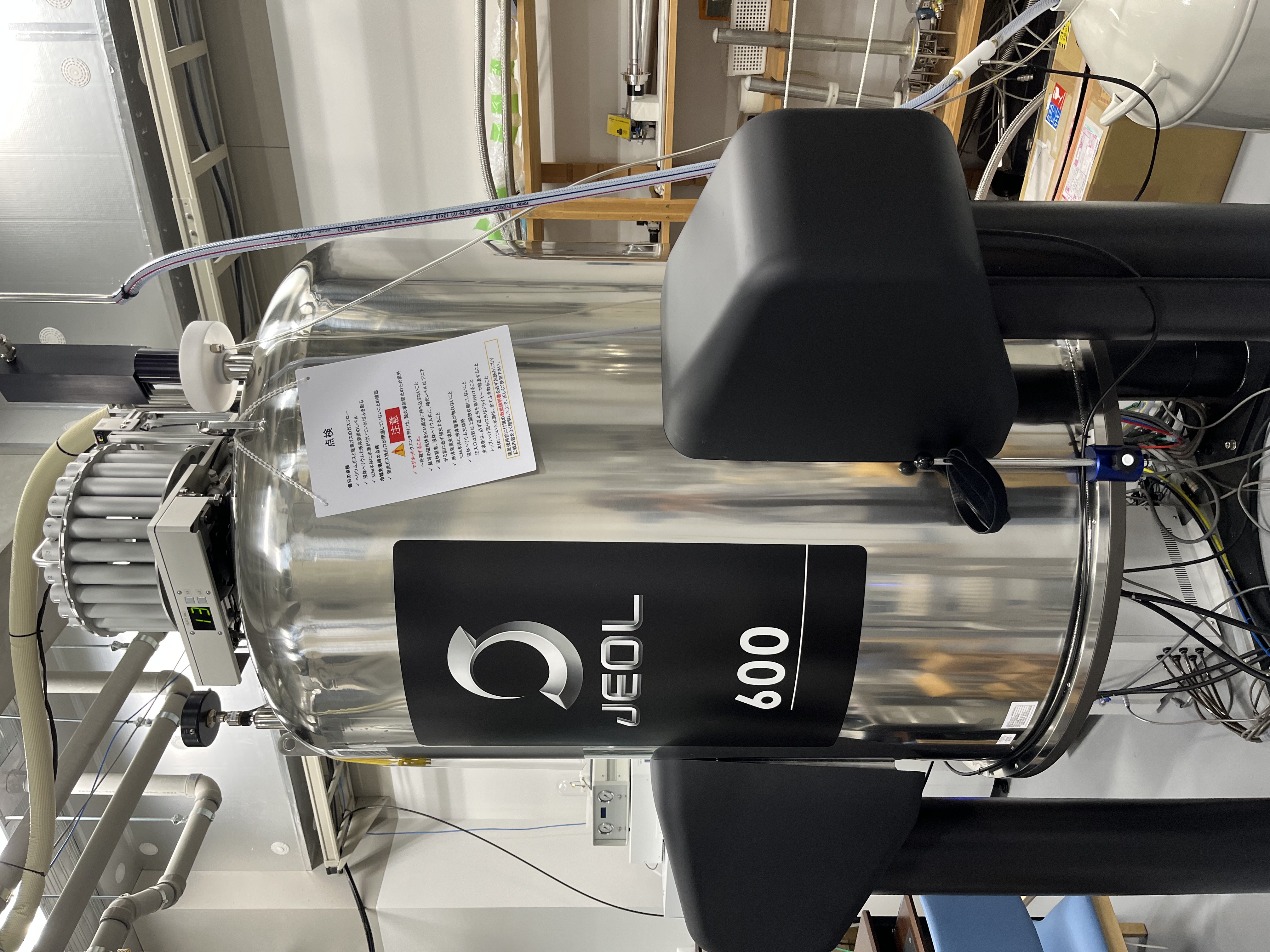
| Model | JEOL, ECZL-600 |
|---|---|
| Magnet | 14T, Bore diameter: 54mm |
| Solid sample measurement (Telemetry compatible) |
Solid(NEW) ・2mmFX/MAS F free probe(number of revolutions 40kHz、-100~+100℃) ・3.2mmAutoMAS probe(number of revolutions 22kHz、-60~+150℃)、Gel measurement possible ・3.2mm wide temperature range HXMAS probe(number of revolutions 22kHz、-100~+200℃)、Gel measurement possible ・Magnetic field application probe for diffusion measurement(2000G/cm@50A) Solid(OLD) ・2.5mm double resonance(1H,31P~15N) ・M-range for solids at room temperature MAS、can rotate up to 15 kHz(7Li, 11B, 29Si, 27Al etc) ・L-range for solids at room temperature MAS、can rotate up to 15 kHz(17O, 137Ba, 10B, 35Cl etc) ・6mmφ probe for Y nucleus for solids at room temperature MAS、can rotate up to 10 kHz ・8mm for low-γ(29Si~25Mg) ・4mm 89Y-1H CP only ・4mm 27Al-1H CP only ・1.3mm Middle range(11B~29Si) ・1mm F free ・1mm F free double resonance(1H-13C) |
| Liquid sample measurement (Telemetry compatible) |
・5mmROYAL HFX double/triple resonance probe with variable temperature(~180℃) ・Magnetic field application probe for diffusion measurement(2000G/cm@50A) |
| Applications | Local structure analysis around atoms is possible for organic and inorganic materials. Even compounds with low crystallinity can be measured, and a horizontal axis that depends on the crystal structure can be obtained. In addition, the diffusion coefficient of battery materials can be obtained regardless of whether they are liquids or solids. |
| Person in charge | Ando* |
| Notes | Please contact the person in charge when you wish to use the equipment. This equipment is managed and operated by the Instrumental Analysis Group on commission from the "Department of Metallurgy, Materials Science and Materials Processing". |
| * Dispatched from Education Support Group to support NMR measurement. | |
NMR (Nuclear Magnetic Resonance) 400MHz
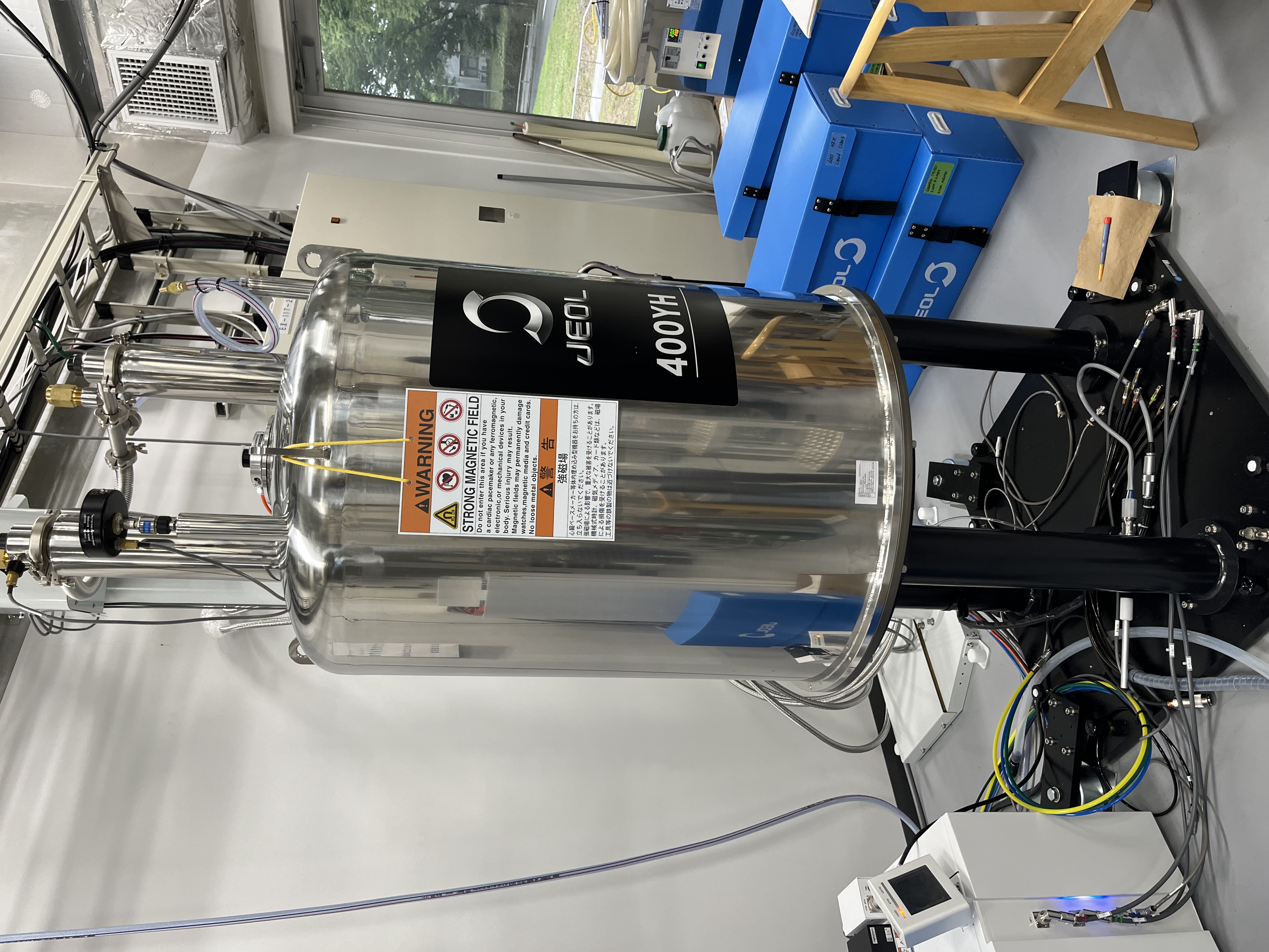
| Model | JEOL, ECZL-400G |
|---|---|
| Magnet | 9.4T, Bore radius: 54mm |
| Solid sample measurement (Telemetry compatible) |
・2mmFX/MAS F free probe(number of revolutions 40kHz、-100~+100℃)、supports MQ-MS measurement ・Magnetic field application probe for diffusion measurement(1200G/cm@30A) ・4mm wide temperature range HXMAS probe(number of revolutions 18kHz、-100~+200℃) ・(-150°C - 150°C, max. rotation speed: 12kHz) |
| Liquid sample measurement (Telemetry compatible) |
・5mmROYAL HFX double/triple resonance probe with variable temperature(~180℃) ・Magnetic field application probe for diffusion measurement(1200G/cm@30A) |
| Applications | Local structure analysis around atoms is possible for organic and inorganic materials. Even compounds with low crystallinity can be measured, and a horizontal axis that depends on the crystal structure can be obtained. In addition, the diffusion coefficient of battery materials can be obtained regardless of whether they are liquids or solids. |
| Person in charge | Ando* |
| Notes | Please contact the person in charge when you wish to use the equipment. This equipment is managed and operated by the Instrumental Analysis Group on commission from the "Department of Metallurgy, Materials Science and Materials Processing". |
| * Dispatched from Education Support Group to support NMR measurement. | |
NMR (Nuclear Magnetic Resonance) 300MHz
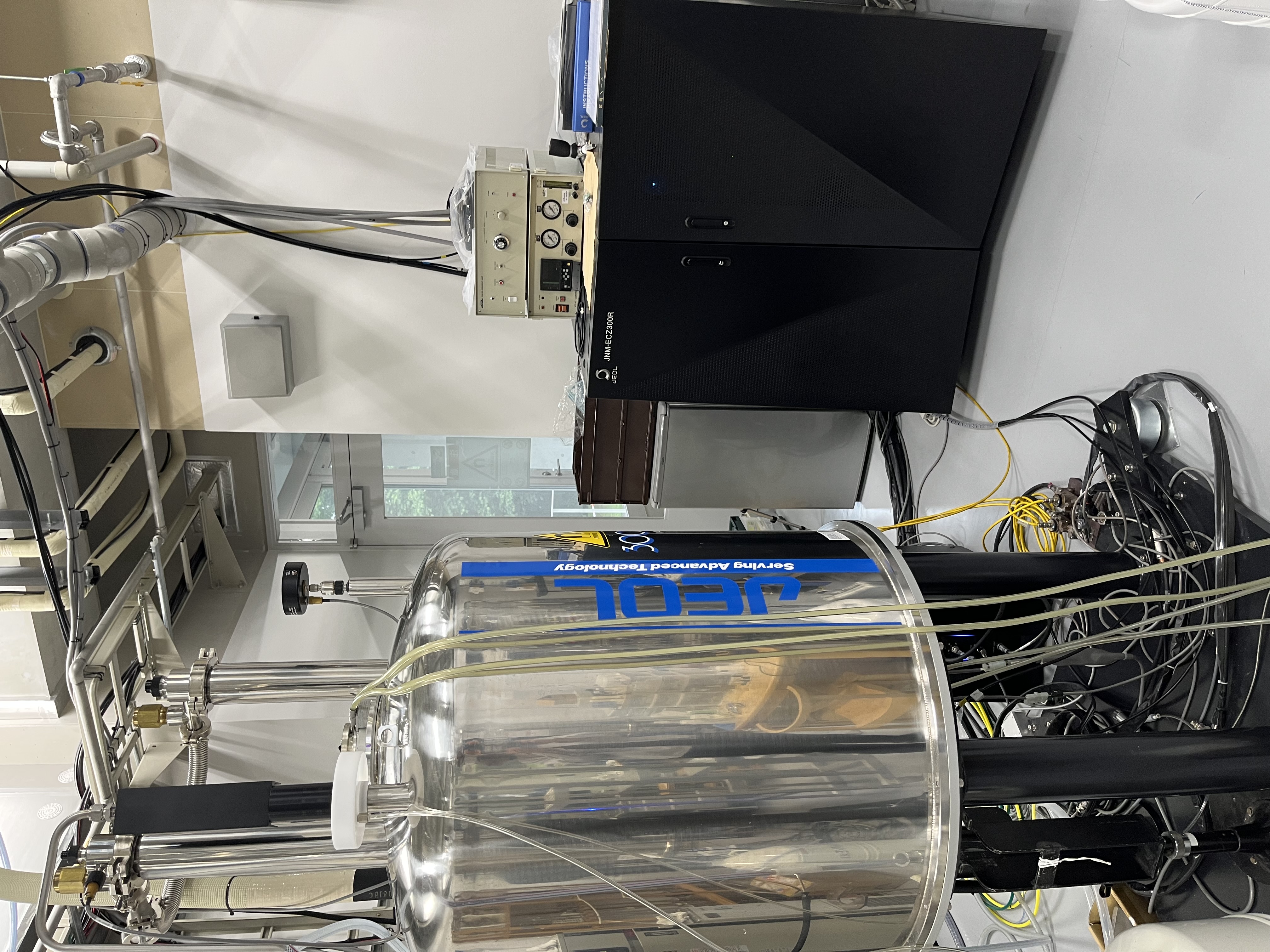
| Model | JEOL, ECZ-300R |
|---|---|
| Magnet | 7T, Bore radius: 89mm |
| Solid sample measurement (Telemetry compatible) |
・4mm High temperature diffusion probe(Diffusion coefficient can be measured from room temperature to 500℃) ・4mmφMAS Probe(13C, 7Li, 31P, 11B etc) ・4mmφHigh temperature laser MAS Probe(Up to 600°C temperature rise possible) |
| Applications | Local structure analysis around atoms is possible for organic and inorganic materials. Even compounds with low crystallinity can be measured, and a horizontal axis that depends on the crystal structure can be obtained. In addition, the diffusion coefficient of battery materials can be obtained regardless of whether they are liquids or solids. |
| Person in charge | Ando* |
| Notes | Please contact the person in charge when you wish to use the equipment. This equipment is managed and operated by the Instrumental Analysis Group on commission from the "Department of Metallurgy, Materials Science and Materials Processing". |
| * Dispatched from Education Support Group to support NMR measurement. | |